How to Reduce Voids in HDI Via Filling
Voids in HDI via filling are commonly caused by trapped air, unsuitable paste rheology, incomplete filling, contamination and uncontrolled curing. Reducing them requires the material, via geometry, filling method and curing profile to be evaluated as one complete process.

Quick answer
The most effective way to reduce via-filling voids is to remove trapped air before curing, match paste rheology to the via geometry, ensure complete bottom-to-top filling and use a controlled curing profile. A high-solid-content conductive paste can reduce volatile-related shrinkage, but filling parameters must still be validated using the actual PCB design.
What Are Voids in HDI Via Filling?
A via-filling void is an unfilled cavity, air pocket or discontinuity inside a filled via. Depending on its position and size, a void can reduce the effective conductive area, increase electrical resistance and interfere with heat transfer through the PCB structure.
In HDI PCBs, the risk becomes more significant because microvias may have small openings, relatively high aspect ratios and limited paths for trapped air to escape. Stacked, staggered, blind and buried structures also place different demands on the filling material and process.
Not every internal feature has the same effect on reliability. Acceptance criteria should be based on the via design, electrical requirements, thermal performance and the customer’s inspection standard.
Six Common Causes of Voids in Conductive Via Filling
CAUSE 01
Trapped Air
Air may remain at the bottom or sidewall of the via when the paste enters too quickly or when there is no effective escape path.
CAUSE 02
Unsuitable Rheology
A paste that is too viscous may not reach the bottom of a narrow via, while a paste that is too fluid may slump or provide poor volume control.
CAUSE 03
Incomplete Filling
Insufficient pressure, filling time, deposited volume or printing passes can leave unfilled regions inside the via.
CAUSE 04
Contaminated Via Surfaces
Moisture, dust, processing residue and surface contamination can affect paste flow, adhesion and curing consistency.
CAUSE 05
Volatile Release
Volatile components or absorbed moisture may form gas during heating. If the gas cannot escape before the paste sets, internal voids can remain.
CAUSE 06
Incorrect Curing Profile
Heating too quickly can trap gases, while insufficient temperature or time can leave the material incompletely cured.

How to Reduce Voids in HDI Via Filling
Confirm the Via Geometry
Record the via diameter, depth, aspect ratio, wall condition and required filling volume. Do not assume that one paste or printing setting is suitable for every HDI structure.
Clean and Dry the Substrate
Remove moisture, dust, oils and process residue before filling. Substrate preparation should be controlled and confirmed before introducing the conductive paste.
Control Paste Condition
Follow the product’s storage and handling instructions. Confirm that the paste is uniform and suitable for use before printing or dispensing. Avoid introducing air during unnecessary high-speed mixing.
Fill from the Bottom Up
The filling method should help air escape as the paste enters. Depending on the via design, vacuum assistance, controlled pressure, optimized squeegee settings or multiple filling passes may be evaluated.
Use a Controlled Curing Profile
Avoid an excessively rapid temperature rise that could trap gas. Start with the supplier’s reference profile, then validate the actual temperature, time and atmosphere using the production substrate and deposited volume.
Inspect Before Mass Production
Use cross-section inspection, X-ray or other suitable methods to evaluate voids, filling completeness and interface quality. Also test resistance, adhesion and thermal-cycle reliability.
HDI Via Filling Troubleshooting Guide
| Observed problem | Possible cause | What to evaluate |
|---|---|---|
| Void at the via bottom | Trapped air or incomplete paste penetration | Filling direction, vacuum assistance, pressure and paste rheology |
| Multiple small internal voids | Air introduced during mixing or volatile release | Paste handling, moisture control, solid content and heating rate |
| Cracks after curing | Shrinkage, thermal mismatch or excessive cure stress | CTE, solid content, cure profile, via dimensions and substrate compatibility |
| High resistance | Incomplete filling, under-curing or poor conductive network formation | Filled volume, curing condition and resistance measurement method |
| Poor adhesion | Contamination or incompatible surface condition | Cleaning, drying, surface preparation and material compatibility |
What to Check When Selecting a Via Filling Paste
A suitable conductive via-filling material should be selected using measurable process and reliability requirements, not conductivity alone.
Evaluate the required resistance of the vertical interconnection.
Important when the via is also part of the heat-transfer path.
Higher solid content can reduce volume loss related to volatile removal.
Must support penetration, air release and controlled deposited volume.
Influence dimensional stability during curing and thermal cycling.
Confirm compatibility with the actual via wall and substrate materials.
Ensure that the required temperature and atmosphere suit the process.
Verify filling quality, resistance, adhesion and thermal-cycle performance.

JUFENG SOLDER MATERIAL SOLUTION
JL-CS-F01 Via Filling Conductive Copper Paste
JL-CS-F01 is a one-component conductive copper paste developed for PCB via filling, HDI conductive plugging and thermal via applications. Its 100% solid-content formulation is designed to reduce volatile content and volume loss during curing.
Material selection alone cannot eliminate every void. Via geometry, substrate preparation, filling equipment, curing conditions and inspection criteria must be evaluated together.
| Property | JL-CS-F01 reference value | Why it matters |
|---|---|---|
| Material type | One-component copper resin | Simplifies preparation and batch consistency |
| Solid content | 100% by TGA | Helps reduce volatile-related volume loss |
| Electrical resistivity | <8×10⁻⁵ Ω·cm | Supports low-resistance conductive via filling |
| Thermal conductivity | 124 W/m·K | Supports heat transfer through filled vias |
| Glass transition temperature | 160–190°C | Relevant to dimensional stability |
| CTE below Tg | 40–50 ppm/°C | Helps manage thermal expansion mismatch |
| Curing reference | 180°C for 60 min under nitrogen | Starting point for process validation |
| Storage and shelf life | −10°C to 10°C / 3 months | Supports controlled material handling |
The listed values are engineering references. Final conditions should be confirmed using the actual via dimensions, substrate, equipment and reliability requirements.
Recommended Applications
HDI Microvia Filling
For selected conductive HDI via and microvia structures after process validation.
Thermal Via Filling
For vertical heat-transfer paths beneath power components and high-heat areas.
Multilayer PCB Structures
For selected blind, buried, stacked or staggered structures after geometry evaluation.
Advanced Packaging Evaluation
TGV and other package-via projects require separate adhesion and reliability testing.
Information to Prepare Before Sample Testing
- Substrate and via-wall materials
- Via diameter, depth and aspect ratio
- Blind, buried, through or microvia structure
- Printing, dispensing or vacuum-filling equipment
- Available curing temperature and atmosphere
- Target resistance and thermal conductivity
- Inspection and reliability requirements
Frequently Asked Questions
Can conductive copper paste completely eliminate via-filling voids?
No material can guarantee zero voids in every structure. Paste properties, via geometry, filling equipment, trapped air, substrate condition and curing control all affect the result.
Does 100% solid content mean zero shrinkage?
It indicates very low volatile content and helps reduce volume loss related to solvent removal. Actual dimensional change still depends on the resin system, curing reaction, deposited volume and process conditions.
Is JL-CS-F01 suitable for every HDI microvia?
No single paste is suitable for every design. Via diameter, depth, aspect ratio, stack-up, filling method and reliability target should be reviewed before approval.
What is the curing condition for JL-CS-F01?
The standard reference is 180°C for 60 minutes under nitrogen. The final profile should be confirmed using the actual substrate, filling volume and production equipment.
Can JL-CS-F01 be evaluated for TGV filling?
Yes, as an evaluation project. Glass type, surface condition, via aspect ratio, filling method, curing compatibility and thermal-cycle reliability must be tested before production use.
REQUEST TDS SAMPLE OR TECHNICAL SUPPORT
Need Help Reducing Voids in Your HDI Via Filling Process?
Send us your substrate, via diameter, via depth, aspect ratio, filling method and curing conditions. The Jufeng Solder team can provide the JL-CS-F01 TDS, sample evaluation and material-selection support.
Email: marketing002@jufengxi.com | WhatsApp: +86 183 1258 2917
Flexible Conductive Copper Paste for Reliable Flexible Electronics
Related Article

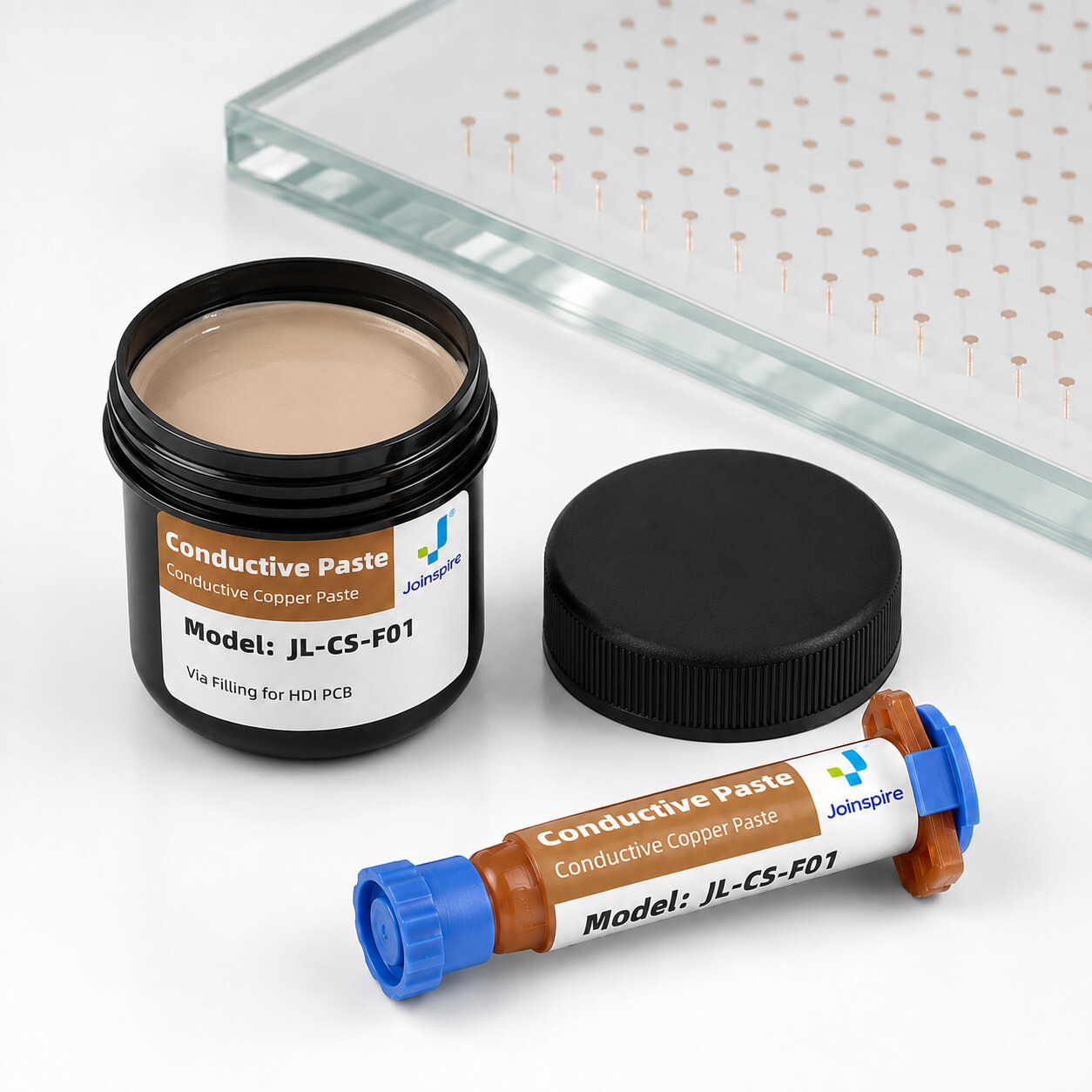
Jufeng JL-CS-F01 copper via filling paste is a single-component conductive resin material developed for via plugging and filling.