


JL-CS-F01 Conductive Copper Paste
JL-CS-F01 Via Filling Copper Paste for HDI PCB
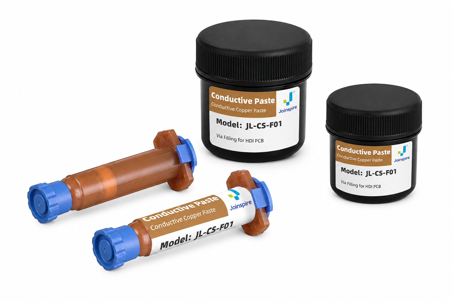
A one-component conductive copper paste developed for PCB via filling, HDI conductive plugging and thermal via applications. It combines high thermal conductivity, low electrical resistivity, low CTE and strong adhesion for reliable vertical interconnections.
What Is Via Filling Copper Paste?
Via filling copper paste—also searched as conductive via fill paste, copper via plugging paste or PCB via filling material—is used to fill selected vias where electrical conduction and heat transfer are required. JL-CS-F01 is formulated for PCB via filling, HDI interconnect structures and electronic packaging processes that require low resistance, controlled thermal expansion and dependable adhesion.
High Thermal Conductivity
Thermal conductivity of 124 W/m·K helps filled vias transfer heat through multilayer PCB and package structures.
Low Electrical Resistivity
Electrical resistivity below 8×10⁻⁵ Ω·cm supports low-resistance vertical interconnection and conductive via plugging.
Low CTE and Dimensional Stability
A CTE of 40–50 ppm/°C below Tg helps reduce expansion mismatch during curing, reflow and thermal cycling.
Crack-Resistant Via Filling
The one-component resin system is designed to reduce cracking in properly filled and cured conductive via structures.
Strong Adhesion
A specified adhesion result of 100/100 supports reliable bonding when the substrate and process are properly prepared.
100% Solids and Halogen-Free
The 100% solids, halogen-free formulation is designed for controlled filling and reduced volatile content during curing.
JL-CS-F01 Technical Specifications
The following values are provided for engineering evaluation. Final process settings must be confirmed according to via diameter, via depth, substrate, filling equipment and reliability requirements.
Recommended Use
Recommended for conductive PCB via filling, thermal via filling, HDI via plugging and selected electronic packaging structures.
The standard curing reference is 180°C for 60 minutes under nitrogen. Confirm the actual profile after evaluating fill depth, deposited volume and production equipment.
Advanced Applications of Via-Filling Copper Paste
JL-CS-F01 is primarily positioned for PCB and HDI via filling. Emerging packaging applications such as TGV and TMV require separate compatibility and reliability evaluation before production use.
HDI Microvia Filling
Conductive copper paste for selected HDI via and microvia structures requiring vertical electrical and thermal paths.
Thermal Via Filling
High-thermal-conductivity via fill for transferring heat from power components through PCB layers.
Any-Layer HDI Interconnects
Potential use in stacked or staggered conductive via structures after geometry, filling and reliability validation.
Electronic Package Via Filling
Conductive filling for selected package substrates and vertical interconnect structures requiring heat transfer and low resistance.
TGV Copper Paste Evaluation
For through-glass via and glass interposer projects, glass adhesion, via aspect ratio, filling method and thermal-cycle reliability must be evaluated.
TMV Filling Evaluation
Through-mold via projects require confirmation of mold-compound compatibility, via dimensions, curing conditions and package-level reliability.
Copper Paste vs. Non-Conductive Via Fill
The correct via-filling material depends on whether the design needs only structural filling or also requires electrical and thermal conduction.
Conductive Copper Paste Via Fill
Designed to provide both electrical connection and enhanced heat transfer through the filled via.
Common evaluation factors include resistivity, thermal conductivity, CTE, adhesion, void control and curing profile.
Non-Conductive Resin Via Fill
Primarily used for structural support, planarization and via protection where direct electrical or high-level thermal conduction is not required.
Material selection should follow the via structure, copper capping process and finished-board reliability requirements.
Via Filling Process Evaluation
Before mass production, evaluate the complete filling and curing process using the actual PCB or package design.
Via Filling Copper Paste FAQ
Frequently asked questions about JL-CS-F01 conductive copper paste and via-filling applications.
What is conductive via filling copper paste used for?
It is used in selected PCB, HDI, thermal via and electronic packaging structures where the filled via must support electrical conduction and heat transfer.
Is JL-CS-F01 suitable for every HDI microvia?
No single material is suitable for every structure. Via diameter, depth, aspect ratio, board stack-up, filling method and reliability target must be evaluated before production.
What is the curing condition for JL-CS-F01?
The standard reference is 180°C for 60 minutes under nitrogen. The final curing profile should be confirmed with the actual deposited volume, substrate and equipment.
Can JL-CS-F01 be used as TGV copper paste?
TGV projects require separate evaluation of glass adhesion, via geometry, filling method and thermal-cycle reliability. Contact us with the glass type and TGV dimensions for technical assessment.
What information is needed for a via-filling sample evaluation?
Please provide the substrate material, via diameter and depth, aspect ratio, filling method, curing equipment, target conductivity and reliability requirements.
Looking for Via Filling Copper Paste?
Send your via dimensions, substrate, filling method and curing conditions. Our team can provide JL-CS-F01 samples, technical evaluation and application support for PCB, HDI and advanced packaging projects.
Want the product? Contact us!
