How to Evaluate SAC305 Solder Paste for Stencil Printing
How to Evaluate SAC305 Solder Paste on Your SMT Line
Start a SAC305 solder paste stencil printing trial with the smallest apertures on your PCB. Measure deposit volume and variation with solder paste inspection (SPI), then check the first prints after a typical line stop. These results help you decide whether a paste is ready for a production trial.
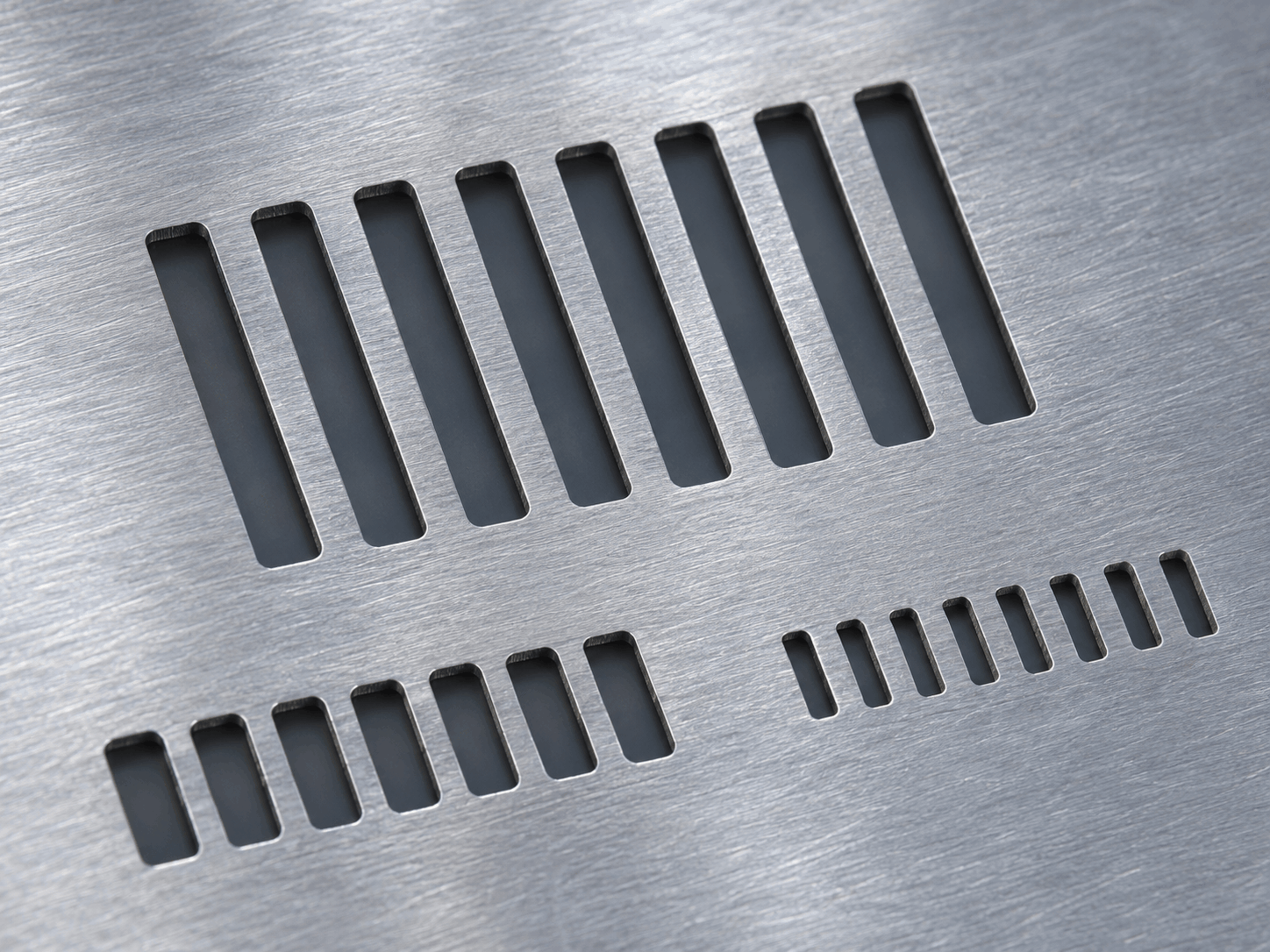
Check Stencil Aperture Area Ratio First
SAC305 is the lead-free alloy Sn96.5Ag3.0Cu0.5. Powder size and flux formulation also influence how a SAC305 solder paste prints. Start by checking the aperture geometry and solder volume required by your PCB before comparing formulations.
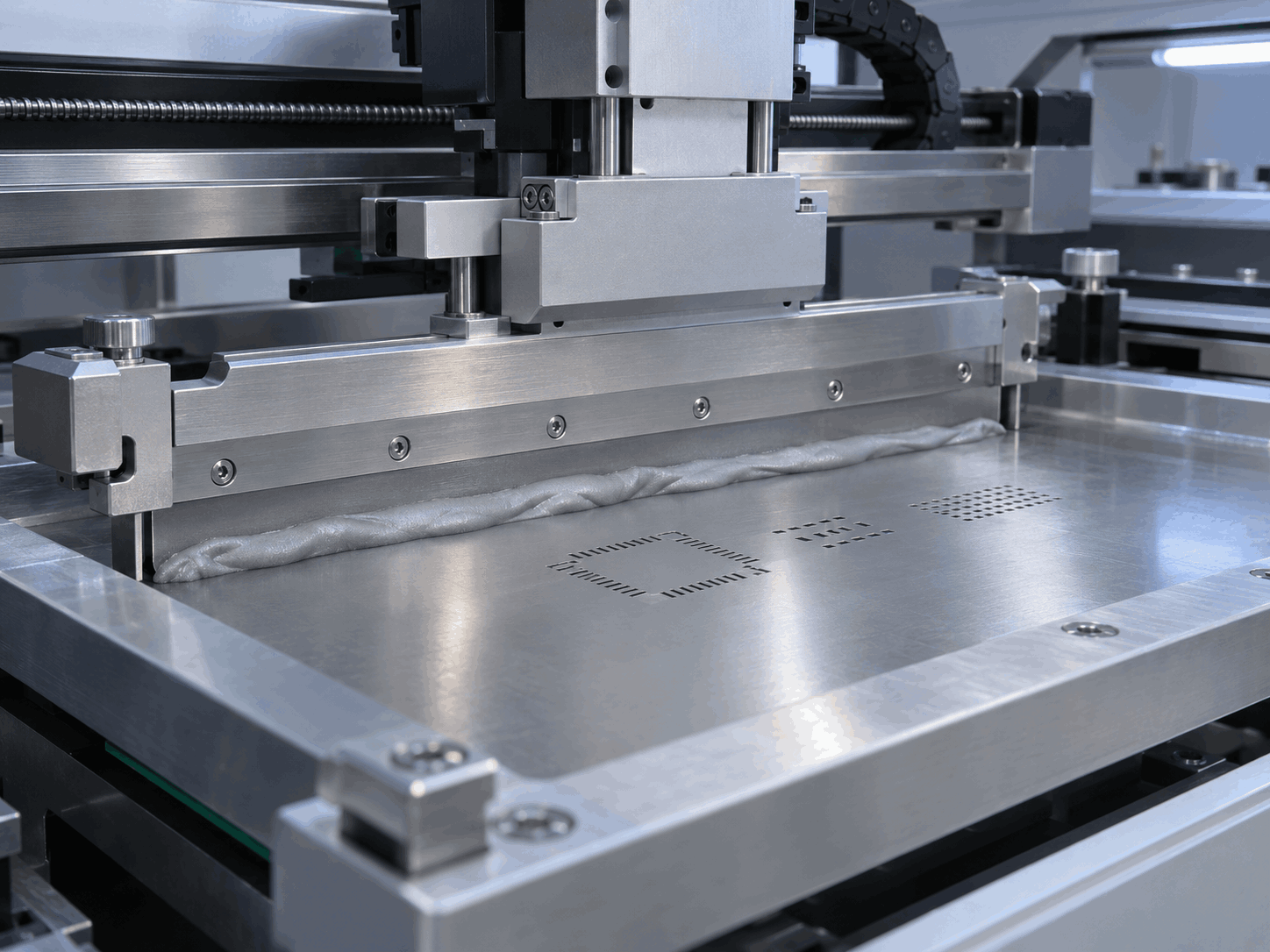
What stencil thickness changes
Area ratio (AR) compares the aperture opening area with the area of its sidewalls. For a rectangular opening of length L and width W in a foil of thickness t, AR = L × W ÷ [2 × t × (L + W)]. Use the same units for all three dimensions.
A 0.20 × 0.25 mm aperture in a 0.10 mm foil has an AR of about 0.56. At 0.075 mm foil thickness, the same aperture is about 0.74, and its theoretical volume drops by 25%. A thinner foil can improve release from small apertures, so verify that larger joints still receive enough paste.
Use 0.66 as a common design guideline. For apertures below that guideline, compare release on the actual board and evaluate options such as foil thickness, aperture finish or a finer powder grade. Stencil print metrics reference.
Run a Controlled SAC305 Stencil Printing Trial
Record the starting conditions
Use the same PCB revision, stencil, board support, blade and SPI program when comparing pastes. Log the paste grade and lot, handling per the TDS, time on the stencil, print speed, blade pressure, separation settings and under-stencil wipe schedule. Clean the stencil between candidates and keep the starting conditions comparable.
Print through a normal cycle
Measure startup and steady-state boards, including prints near the end of the normal wipe interval. Pause for a duration representative of the line, then record the first board and subsequent prints until volume returns to the steady-state range. Note whether the printer wiped before restart. Response-to-pause reference.
Compare the same aperture groups
Group SPI readings by aperture size and shape. Include the smallest openings, fine-pitch pads and any larger deposits critical to joint formation. Compare mean volume, variation, offset and defect counts against the limits set for the assembly, with post-pause results shown separately.
Use SPI Data to Calculate Transfer Efficiency
Transfer efficiency (%) = SPI-measured paste deposit volume ÷ theoretical stencil aperture volume × 100. Theoretical volume is the aperture opening area multiplied by stencil thickness for a straight-walled opening.
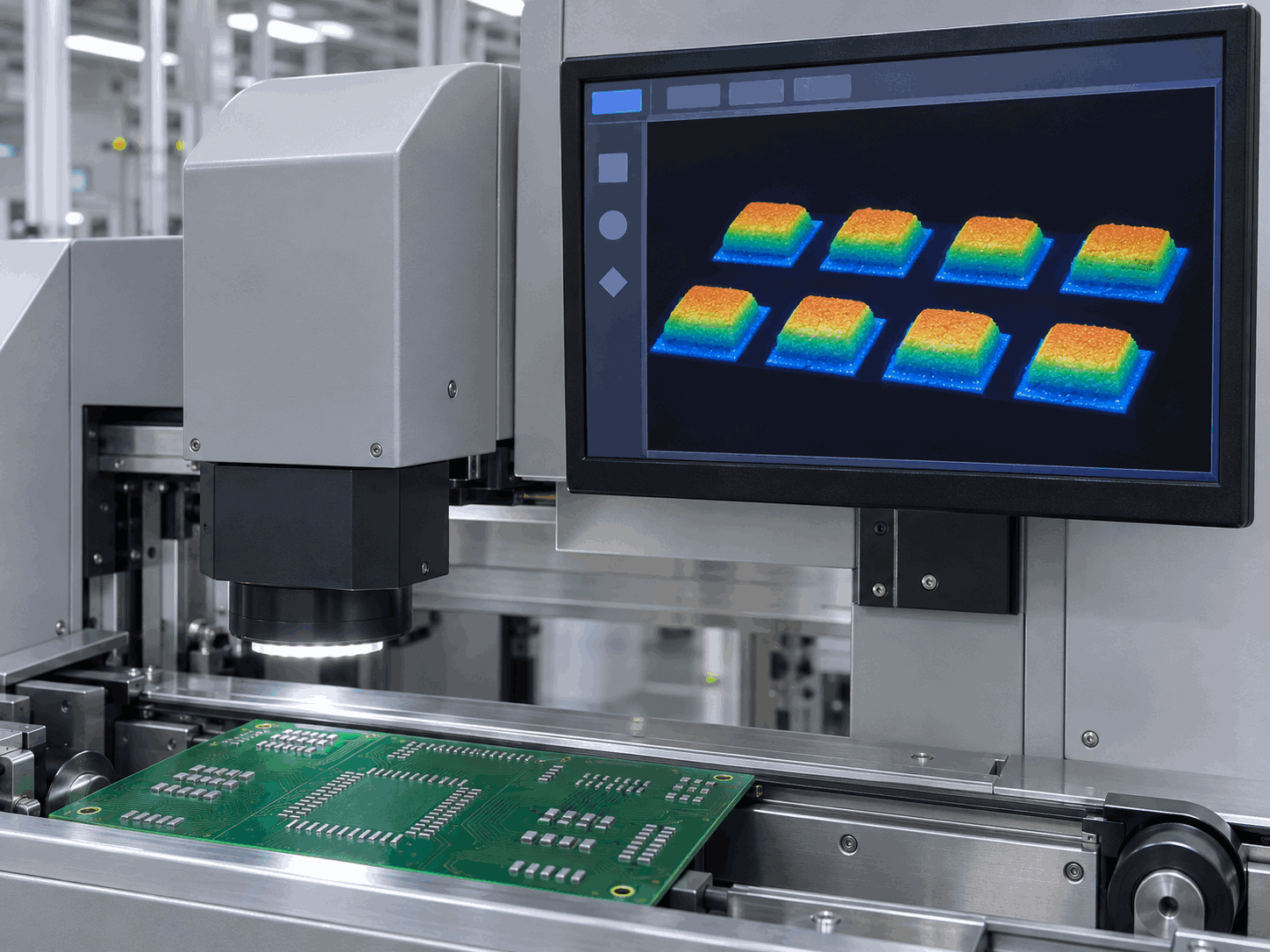
Use transfer efficiency to compare release. Check deposit volume and offset against your pad-level SPI limits, and track variation across prints. A line-wide average can hide repeated low deposits on the smallest BGA or fine-pitch pads.
Troubleshoot SMT Stencil Printing Defects
Use the defect location and print sequence to identify likely causes. Set blade pressure to the minimum that gives a clean wipe, then vary one parameter at a time or use a planned experiment. Stencil printer setup reference.
| SPI or visual signal | Check first | Next action |
|---|---|---|
| Low or variable volume on small pads | Low area ratio, blocked apertures or irregular release. | Review the smallest aperture dimensions and inspect the stencil. Check SPI immediately before and after a clean wipe. Then test a controlled change to PCB-to-stencil separation speed. |
| Paste bridging or smearing | Paste on the stencil underside, poor board-to-stencil contact or print misalignment. | Inspect the underside, check tooling support and fiducial alignment, and confirm blade pressure is just sufficient for a clean stroke. Compare defect counts after correcting the identified condition. |
| Bad first print after a pause | Paste response to pause or an inconsistent restart and wipe sequence. | Compare pre-pause volume with the first several prints after restart. Record recovery prints and evaluate the restart procedure using an equivalent pause. |
SAC305 Solder Paste Printing FAQ
Which powder grade should I test for fine-pitch printing?
Use the minimum aperture dimensions, area ratio and supplier guidance to choose a baseline grade. T4 or T5 may be candidates when T3 prints inconsistently through the smallest apertures. Verify deposit volume, variation and post-pause recovery on the actual assembly.
What should I lock before releasing the print process?
Record the approved paste grade, printer settings, wipe schedule, pause-and-restart procedure and SPI limits by pad group. Carry representative boards through placement and reflow to confirm solder joint quality before releasing the process.
Request Jufeng SAC305 Solder Paste for a Line Trial
Jufeng supplies no-clean SAC305 solder paste in T3, T4 and T5 powder grades. Send your minimum aperture dimensions, stencil thickness, PCB finish and target cycle time. If you are troubleshooting a print issue, include the relevant SPI readings or a pad image. We can help you choose a grade to evaluate and provide the corresponding technical data sheet (TDS). View Jufeng SAC305 solder paste specifications.
Large-Area Silver Sintering: From Stable Printing to Thermal Performance
Related Article