qr Code Url

Scan qrcode to view mobile website

Data is empty
0
Member Center
Exit
    Home /Applications /Product Updates /Via-Fill Conductive Copper Paste: How JL-CS-F01 Solves Through-Hole Filling Challenges in Semiconductor Packaging /

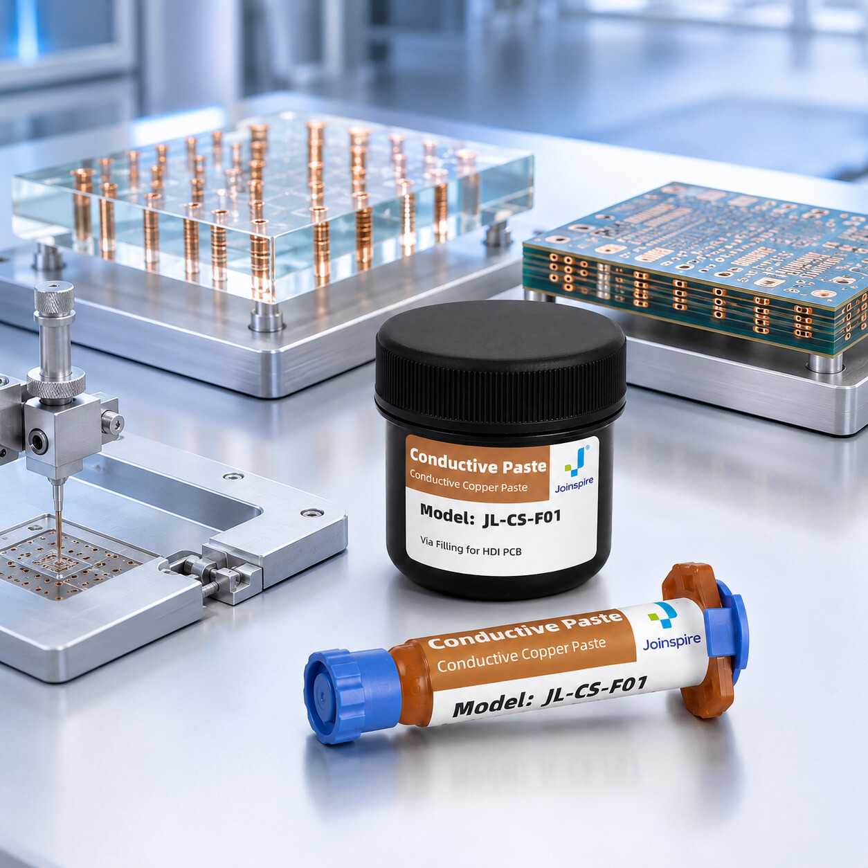
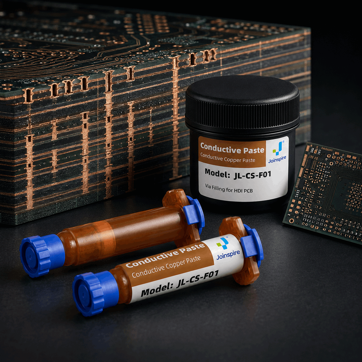
    Via-Fill Conductive Copper Paste: How JL-CS-F01 Solves Through-Hole Filling Challenges in Semiconductor Packaging

    2026-07-09

    A single-component via-fill resin engineered for low CTE, high conductivity, and process flexibility.


    Industry pain points: why do via-fill materials keep failing?

    In advanced semiconductor packaging, PCB via-filling, and microelectronic interconnection processes, engineers repeatedly run into the same set of problems:

    Cracking failures
    Conventional fill materials often have a high coefficient of thermal expansion (CTE), making them prone to micro-cracking during thermal cycling or 260°C reflow — compromising the conductive path and causing batch-level yield loss.
    Inconsistent conductivity
    Some conductive pastes cure with uneven or elevated resistivity, degrading signal integrity and overall thermal dissipation.
    Weak adhesion
    Poor bonding between the fill material and via wall substrate leads to delamination or peeling after repeated thermal cycling.
    Compliance risk
    Halogen-containing materials struggle to meet RoHS and halogen-free requirements, which can jeopardize export certification and customer qualification.
    Limited process compatibility
    Materials restricted to a single application method (dispensing-only or printing-only) force costly line reconfiguration when switching processes.

    These issues usually trace back to a mismatch between the resin's thermal expansion behavior, its curing chemistry, and the conductive filler system — a detail that's easy to overlook during material selection but ultimately determines production yield.

    JL-CS-F01: solving via-fill challenges at the material level

    Developed by Joinspire, JL-CS-F01 is a single-component via-fill conductive resin engineered specifically to address the pain points above:

    ✓
    Low CTE, excellent dimensional stability — CTE α1 (below Tg) of 40-50ppm, CTE α2 (above Tg) of 110-130ppm, with total expansion at 260°C of only 1.5-2.0%, significantly reducing thermal-stress-induced cracking.
    ✓
    High electrical conductivity — Resistivity below 8×10⁻⁵ Ω·cm, suitable for high-density interconnect signal transmission requirements.
    ✓
    High thermal conductivity — Thermal conductivity of 124 W/m·k, improving heat dissipation, particularly valuable for power device packaging.
    ✓
    Excellent adhesion — 100/100 rating under cross-hatch + 3M tape testing, minimizing long-term delamination risk.
    ✓
    Halogen-free, environmentally compliant — Meets mainstream international electronics manufacturing environmental standards.
    ✓
    Low-temperature curing — Fully cures at 170-190°C in 60-90 minutes, compatible with a wide range of temperature-sensitive substrates and production line cycle times.
    ✓
    Dual process compatibility — Works with both dispensing and printing processes, offering flexibility across different production line setups without requiring equipment changes.

    Applications

    1
    Advanced semiconductor packaging via-fill (TSV/TGV-type applications)
    2
    PCB blind/buried via conductive fill
    3
    Power module thermal pathway construction
    4
    Microelectronic device interconnection and structural reinforcement
    5
    Chip-level packaging gap-fill and structural support

    Key technical specifications

    Property Value Test method
    Appearance Light brown Visual
    Viscosity 5-30 Pa.s @20rpm, Viscometer
    Solid content 100% TGA
    Resistivity <8×10⁻⁵ Ω·cm 4-point probe method
    Thermal conductivity 124 W/m·k Laser flash method
    Glass transition temperature (Tg) 160°C-190°C TMA
    CTE (below Tg) α1 40-50ppm TMA
    CTE (above Tg) α2 110-130ppm TMA
    Total expansion at 260°C 1.5-2.0% TMA
    Adhesion 100/100 Cross-hatch + 3M tape method
    Curing condition 170-190°C, 60-90min Atmosphere: N₂ or air
    Storage temperature -10~10°C —
    Shelf life 3 months —

    Usage & process guidelines

    Storage
    Store at -10~10°C, protected from light, and avoid high-humidity environments.
    Thawing
    After removal from cold storage, let the material sit at room temperature (25°C) for at least 4 hours to fully thaw, then wipe off any surface moisture before use.
    Process application
    Compatible with dispensing and printing processes for via-fill, gap-fill, and similar applications. Cure in an oven at 170-180°C for 60-90 minutes under nitrogen or air atmosphere.

    FAQ

    What packaging processes is JL-CS-F01 suitable for?
    It's designed for advanced semiconductor packaging via-fill, PCB blind/buried via conductive fill, and power module thermal pathway construction, and is compatible with both dispensing and printing processes.
    How does copper paste compare to traditional silver conductive paste?
    Copper paste delivers strong conductivity and thermal performance at a lower material cost than silver-based alternatives, making it well-suited for cost-sensitive, high-volume production while still meeting demanding electrical and thermal requirements.
    Does this product meet environmental compliance requirements?
    Yes — it is halogen-free and meets mainstream environmental compliance standards for electronics manufacturing.
    Is the cured material prone to cracking?
    The low CTE and strong dimensional stability, combined with the recommended curing profile (170-190°C, 60-90 minutes), significantly reduce cracking risk during thermal cycling and reflow processes.
    What is the product's shelf life?
    3 months when stored at -10~10°C, protected from light. Purchasing planning should account for batch-based inventory turnover.
    Share:

    The Real Bottleneck in AI Chip Packaging Isn’t Compute — It’s Heat

    CP-500FE Flexible Conductive Carbon Paste for Flexible Electronics Applications

    Related Article
    image
    If a 0201 component, miniature sensor lead or tiny PCB pad keeps flooding with solder, the problem may not be your hand, your iron or your temperature setting. The solder wire itself may simply be too thick for the joint.
    Why Can’t I Solder Tiny SMD Components? 0.1mm Ultra-Fine Solder Wire Explained
    2026-07-22
    image
    As AI accelerators move beyond the kilowatt threshold, thermal management is becoming one of the most important challenges in advanced semiconductor packaging.
    The Real Bottleneck in AI Chip Packaging Isn’t Compute — It’s Heat
    2026-07-15
    image
    With the rapid development of flexible electronics including RFID tags, flexible sensors and wearable devices, printing processes based on PET & PI substrates have achieved great progress. However, traditional conductive pastes still have obvious defects in mass production: weak adhesion, cracking after bending, unstable resistance and high comprehensive cost, restricting product upgrading.
    CP-500FE Flexible Conductive Carbon Paste for Flexible Electronics Applications
    2026-06-17
    image
    As new energy vehicles, 5G communication and high-power electronics continue to grow, sintered silver is becoming an important next-generation die attach material for high-reliability electronic packaging.
    This Type of SiC Packaging Material Is Expected to Grow 700%, and Domestic Manufacturers Are Already Taking the Lead
    2026-05-27

    HOME

    About us

    news

    connect us

    SiteMap
    Copyright © 2021 King Theme v2. Powered by web
    京公网安备 32058302002032号
    (387759)
    0