The Real Bottleneck in AI Chip Packaging Isn’t Compute — It’s Heat
This article examines why the die-attach material between the semiconductor die and substrate plays a critical role in heat dissipation, thermal-cycling reliability and the long-term performance of AI and HPC packages.

Rising AI Chip Power Is Changing the Packaging Challenge
Every generation of AI accelerators arrives with a larger power number attached to it. NVIDIA’s H100 operates at around 700 W, while B200- and B300-class devices are expected to move beyond 1,000 W per chip. Once high-bandwidth memory stacks and supporting components are included, industry roadmaps are already pointing toward multi-kilowatt module-level power envelopes.
Most discussions about AI chip thermal management immediately turn to direct liquid cooling, immersion systems, cold plates and microfluidic channels. These technologies are essential, but they address only the visible half of the heat-transfer problem.
The less-discussed thermal bottleneck sits directly beneath the semiconductor die: the bond between the chip and its substrate.
Before heat can reach a cold plate or liquid-cooling system, it must first move through the die-attach layer. If this interface has excessive thermal resistance or poor cycling reliability, improvements elsewhere in the cooling architecture may not fully solve the package-level problem.
Why the Die-Attach Layer Matters More Than It Used To
As AI chip power density increases, three thermal and mechanical challenges intensify at the same time:
Higher Heat Flux
More heat must be transferred out of a smaller footprint and moved through the semiconductor package more quickly.
Greater Cycling Stress
Repeated heating and cooling place greater mechanical stress on every interface within the package stack.
CTE Mismatch
Differences in thermal expansion between silicon, substrate and bonding materials become increasingly difficult to ignore.
Traditional solder die attach was developed for a lower-power era. Its thermal conductivity may represent only a fraction of what modern high-power semiconductor dies require. Under sustained thermal cycling, the solder joint can also become one of the earliest locations for reliability problems.
Common failure mechanisms include void growth, fatigue cracking and delamination. Each of these can increase thermal resistance, reduce mechanical integrity and shorten the service life of the package.

Why Sintered Metal Is Entering the AI and HPC Packaging Conversation
Sintered metal die attach is already widely used in high-performance SiC and GaN power modules for electric vehicles. It is now receiving serious attention from teams developing high-power AI accelerators and high-performance computing packages.
A sintered silver or copper layer is fundamentally different from a conventional solder joint. During the sintering process, metal particles form a highly connected, near-dense metallic bond at a moderate processing temperature. The resulting interface provides a more direct thermal path and stronger resistance to fatigue under repeated thermal cycling.
What “Good” Looks Like in Practice
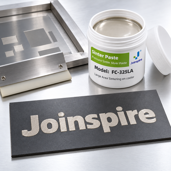
As a die-attach material reference, our JF-PMAg02 pressure-sintered silver paste is designed to create a high-performance metallic bond for applications where heat transfer and long-term interface reliability are critical.
Thermal conductivity
Electrical resistivity
Coefficient of thermal expansion
Typical pressure-sintering conditions
Material values shown above are reference specifications. Actual process performance may vary according to substrate metallization, die size, bond-line thickness, atmosphere and sintering profile.
Different Packaging Processes Require Different Material Routes
Selecting a sintering paste is not simply a matter of choosing the material with the highest thermal conductivity. Equipment capability, applied pressure, processing atmosphere, package design, cost and production volume all affect the most appropriate solution.
Pressure-Sintered Silver Die-Attach Paste
Designed for high-performance die attach where pressure-sintering equipment is available and maximum thermal and reliability performance is required.
View JF-PMAg02 pressure-sintered silver pastePressureless Silver Sintering Paste
Provides thermal conductivity above 200 W/m·K without requiring applied pressure during bonding, offering a more accessible route for prototyping, process evaluation and lower-volume production.
View JF-PMAg01 pressureless silver sintering pastePressure-Sintered Copper Die-Attach Paste
Offers thermal conductivity above 180 W/m·K and provides a competitive alternative where silver cost, availability or supply-chain sensitivity is a concern.
View FC-100U pressure-sintered copper paste

The Practical Question Is Not Simply “Sintering or Solder?”
For engineers developing next-generation power devices, AI accelerators or HPC packages, the practical question is whether the current die-attach material can keep pace with chip power over the next two or three design cycles.
If thermal resistance or cycling reliability is already becoming a design constraint, the die-attach layer deserves review before the next device generation raises heat flux and interface stress even further.
Process requirements can differ significantly between power modules and AI or HPC packages. Pressure capability, atmosphere control, metallization, die size, substrate structure and production volume all affect the most suitable material route.
Key questions to review before selecting a die-attach material
- What junction temperature and thermal resistance targets must the package achieve?
- Is pressure-sintering equipment available on the production line?
- What metallization is used on the die and substrate surfaces?
- What thermal-cycling and power-cycling lifetime is required?
- How sensitive is the project to silver cost or supply-chain risk?
- What bond-line thickness and voiding level can the package tolerate?
Frequently Asked Questions About AI Chip Die Attach
Why is die attach important in AI chip packaging?
The die-attach layer forms the thermal and mechanical connection between the semiconductor die and its substrate. Its thermal resistance, fatigue resistance and coefficient of thermal expansion can directly affect chip temperature and package reliability.
How does sintered metal die attach compare with solder?
Sintered silver and copper can provide higher thermal conductivity and stronger resistance to thermal-cycling fatigue than conventional solder die-attach materials. Actual performance depends on the package structure and bonding process.
Should AI packaging use sintered silver or sintered copper?
The choice depends on thermal targets, cost, metallization, production atmosphere, bonding pressure and long-term reliability requirements. Silver offers very high thermal performance, while copper may provide cost and supply-chain advantages.
Can pressureless sintering be used for prototyping?
Pressureless silver sintering can provide a more accessible route for laboratory evaluation, prototyping and lower-volume production where pressure-sintering equipment is not available.
Working Through a Die-Attach Challenge?
We welcome discussions with teams developing high-power semiconductor packages. Share your substrate metallization, die size, thermal target, bonding conditions and reliability requirements so that the most suitable silver or copper sintering route can be evaluated.
Discuss Your Die-Attach RequirementsWhy Can’t I Solder Tiny SMD Components? 0.1mm Ultra-Fine Solder Wire Explained
Via-Fill Conductive Copper Paste: How JL-CS-F01 Solves Through-Hole Filling Challenges in Semiconductor Packaging
Related Article