Joinspire Brings Advanced Electronic Interconnect Materials to CPCA Show Plus 2026
EXHIBITOR SPOTLIGHT · CPCA SHOW PLUS 2026
As the PCB and semiconductor advanced-packaging industry moves toward higher reliability and greater domestic self-sufficiency, high-performance interconnect materials have become the key to breaking through. Guangdong Joinspire Technology Co., Ltd. will showcase its full product lineup at Booth 6C23, helping manufacturers raise quality, boost efficiency and cut costs across the interconnect process.

At a glance
About the Exhibitor
Guangdong Joinspire Technology Co., Ltd. ("Joinspire") has spent years deepening its expertise in electronic interconnect materials, building an independent portfolio of core IP with fully self-controlled technology. The company holds multiple authoritative certifications, including ISO 9001 and IATF 16949. Backed by stable product quality, mature manufacturing processes and large-scale production capacity, Joinspire has earned broad recognition across the industry and among upstream and downstream customers alike.
Its products span core tracks including precision PCB manufacturing, new-energy vehicles, photovoltaic energy storage, AI data centers and power semiconductor packaging — delivering highly reliable, high-performance, domestically produced material solutions for China's advanced electronics manufacturing and semiconductor industries, and helping the supply chain move toward greater self-sufficiency and higher quality.
 Image placeholder: Joinspire clean-room production / R&D lab
Exhibit Highlights
At this show, Joinspire is focusing on the pain points of high-end PCB and power semiconductor processes, featuring its flagship product — via-fill copper paste JL-CS-F01 — alongside a full supporting lineup that includes PCB trace-repair copper paste and low-temperature sintering materials, addressing production and R&D needs across a wide range of scenarios.

Conductive Paste Series
1. Via-Fill Copper Paste JL-CS-F01 (Flagship Product)
JL-CS-F01 is Joinspire's core material developed for high-density interconnects in advanced PCBs and packaging processes. It is compatible with through-holes, blind vias, HDI micro-vias, TGV through-holes and other mainstream processes, and can replace traditional resin via-fill and electroplated-fill methods — directly resolving common mass-production pain points such as voids inside vias, dimpling at via openings, resistance fluctuation, poor reflow resistance and thermal-expansion cracking. Overall performance is on par with leading international standards.
KEY ADVANTAGE
Mass-Production Compatibility
Supports a low-temperature, fast-curing process that sharply reduces curing shrinkage stress, eliminating board-cracking risk at the source. Compatible with FR4 and high-frequency, high-speed boards; supports both dispensing and printing fill methods with a directly solderable cured surface.
KEY ADVANTAGE
Thermal & Electrical Performance
Forms a continuous, uniform, highly stable conductive and thermal pathway once cured, with a thermal conductivity of up to 124 W/(m·K) — quickly dissipating heat inside vias and preventing localized heat build-up.
KEY ADVANTAGE
Proven Reliability
After multiple rounds of rigorous testing simulating real production conditions, JL-CS-F01 maintained zero voids and zero cracks even after 12 reflow-soldering cycles, delivering industry-leading heat and reflow resistance.
KEY ADVANTAGE
Broad Qualification
Already in mass-production trials with several leading PCB and semiconductor packaging manufacturers, and widely used in HDI boards, TGV through-hole boards and high-frequency, high-speed boards — offering a clear advantage for domestic substitution.
| Property | JL-CS-F01 | Why it matters |
|---|---|---|
| Thermal conductivity | Up to 124 W/(m·K) | Fast heat dissipation, no localized heat build-up |
| Reflow reliability | 0 voids / 0 cracks after 12 reflow cycles | Industry-leading heat and reflow resistance |
| Board compatibility | FR4, high-frequency & high-speed boards | Fits mainstream and advanced substrates |
| Fill methods | Dispensing or printing | Flexible for different production lines |
| Cured surface | Directly solderable | Fits industrial mass-production tempo |
| Applicable processes | Through-hole, blind via, HDI micro-via, TGV | Covers mainstream and advanced packaging |
2. PCB Trace-Repair Conductive Copper Paste JL-CS-C03
Developed specifically for repairing broken traces on circuit boards, this paste delivers 5B adhesion and stable conductivity, is easy to print, and can quickly and precisely repair fine, delicate traces. It significantly lowers PCB scrap rates and saves considerably on production materials and cost — well suited to precision board repair, small-batch rework and prototype development.

Low-Temperature System-Level Sintering Series
This series targets large-area substrate interconnects, module-to-heatsink bonding and other system-level packaging applications. It enables highly reliable metal interconnects under low-temperature process conditions — protecting heat-sensitive components while keeping pace with efficient mass production, balancing process safety with manufacturing efficiency.
SINTERED COPPER
FC-200U-LA
A system-level "copper-for-silver" interconnect solution that maintains excellent electrical and thermal conductivity while significantly easing cost pressure from silver-price volatility — a preferred, cost-saving choice for large-area sintering in high-power modules.
SINTERED SILVER
FC-325LA
Low-temperature, pressureless sintered silver delivering excellent thermal and electrical conductivity after sintering and withstanding high operating temperatures — well suited to high-power chips and third-generation semiconductor device packaging, meeting the long-term reliability demands of high-power-density devices.
Pressure-Assisted Chip-Level Sintering Series
Designed for SiC/GaN high-end power-chip die-attach applications, this series offers both cost-optimized and performance-optimized options, giving customers the flexibility to choose based on their process needs and product positioning — suitable for automotive-grade and industrial-grade, highly reliable packaging.
PRESSURE-SINTERED COPPER
FC-100U
A chip-level, pressure-sintered copper paste that forms a dense copper interconnect layer after sintering, with high thermal conductivity and strong interfacial bonding at a clear cost advantage — widely used for die-attach interconnects in power chips, IGBTs and similar devices.

PRESSURE-SINTERED SILVER
PMAg02
A high-performance, pressure-sintered silver paste that achieves high density and excellent shear strength with low thermal resistance after sintering — a mainstream interconnect material for highly reliable power-semiconductor packaging, suitable for automotive-grade and industrial-grade, high-power device packaging.

A One-Stop Interconnect Material Solution
Backed by a full-spectrum product matrix, Joinspire focuses on power semiconductor packaging and high-end PCB interconnects, building a one-stop material solution centered on "low cost, high thermal conductivity and high reliability." Compared with traditional imported materials, Joinspire's products help customers improve production efficiency, lower overall manufacturing costs and significantly shorten R&D and validation cycles — supporting the industry's move away from import dependence and toward domestic upgrading.

Frequently Asked Questions
What is CPCA Show Plus 2026?
2026 CPCA Show Plus — the Electronic Semiconductor Industry Innovation & Development Summit and International Electronic Circuits (GBA) Exhibition — is a major PCB and electronics-industry trade show taking place October 27–29, 2026 at the Shenzhen World Exhibition & Convention Center (Bao'an).
Where is Joinspire's booth located?
Joinspire will be at Booth 6C23. See the booth guide image on this page, or contact us in advance to schedule a meeting time.
What products will be on display?
The flagship product is via-fill copper paste JL-CS-F01, alongside PCB trace-repair copper paste JL-CS-C03, the low-temperature system-level sintering series (FC-200U-LA, FC-325LA) and the pressure-assisted chip-level sintering series (FC-100U, PMAg02).
Can I schedule a meeting before the show?
Yes — reach out by email or WhatsApp using the contact details below and the Joinspire team will arrange a time to meet at Booth 6C23.
CPCA SHOW PLUS 2026 · OCT 27–29 · BOOTH 6C23
Join Us at Booth 6C23!
A major industry gathering, right here in Shenzhen! We warmly welcome PCB industry professionals, engineers and procurement teams to visit Joinspire at Booth 6C23 for face-to-face technical exchange and partnership discussions — and to explore the future of advanced electronic interconnect materials together.
Email: marketing002@jufengxi.com | WhatsApp: +86 183 1258 2917
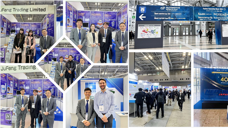
Kickoff Success for the New Year! Jufeng Shines at NEPCON JAPAN
Related Article