


JF-PMAg02 Pressure Sinter Silver Paste
JF-PMAg02 Pressure Sinter Silver Paste
A pressure-assisted silver sinter paste for power-device die attachment, combining stable printing with high thermal conductivity, low resistivity and a dense silver bond layer.
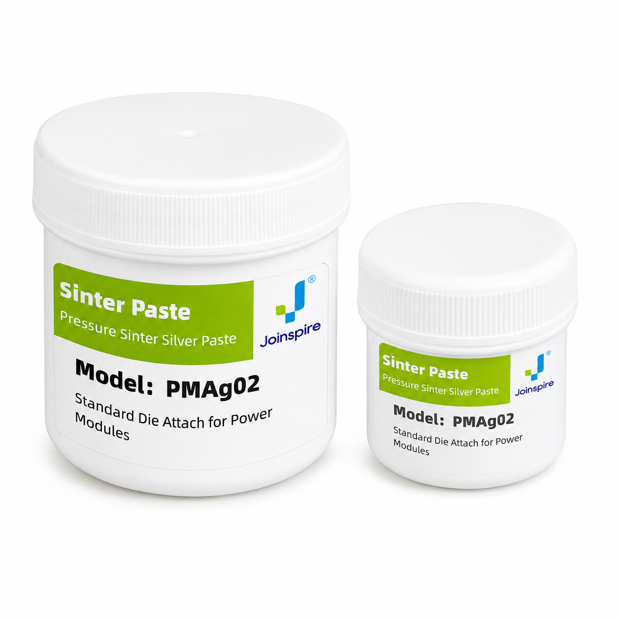
Fast pressure silver sintering for high-power devices
JF-PMAg02 is formulated for pressure sintering in semiconductor packaging. After sintering, the silver layer is uniform and dense, supporting reliable heat transfer and electrical connection for high-power chips.
High Thermal Conductivity
Specified thermal conductivity exceeds 200 W/m·K.
Low Electrical Resistivity
Specified resistivity is below 6 μΩ·cm.
Short Sintering Cycle
Reference pressure-sintering time is 3–5 minutes.
Stable Printing Performance
Supports extended stencil-printing operations with controlled rheology.
Ag / Au / Cu Compatibility
Applicable to common die-attach metallizations with the proper atmosphere.
REACH & RoHS Support
The TDS identifies the material as REACH and RoHS compliant.
Product Specifications
Technical data for engineering evaluation. Final process settings should be confirmed against the selected substrate, package dimensions and production equipment.
Recommended Use
Recommended for pressure-assisted die attachment in power semiconductor and high-power electronic packages. Reference pressure-sintering conditions are 250–270°C, 10–20 MPa and 3–5 minutes; use nitrogen for copper surfaces and confirm the final profile for the actual package.
Typical Applications
Application suitability should be confirmed against substrate finish, material dimensions, processing atmosphere and reliability requirements.
Need JF-PMAg02 for pressure silver sintering?
Provide the chip size, surface finish, bond-line target and pressure-sintering equipment for process review.
Want the product? Contact us!
